Preamplifiers
Preamplifier Short Form Catalog in PDF Format
Preamplifiers
This section describes the amplifier circuits recommended for Judson detectors. The PA-5, PA-6, PA-7 and PA-9 series preamplifiers are current gain amplifiers recommended for photovoltaic detectors and applications. Voltage mode preamplifiers, for use with our photoconductive detectors, include the PA-101 and PA-8200 series preamps. Some general information on our preamplifiers follows:
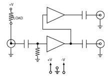
Noise Sources: Figure 1 shows the various noise sources of the detector/preamp system. Values for the preamp noise sources en, in, Vos and ib are listed in the specification tables for each Judson current-mode preamplifier. The preamp noise sources, together with the detector characteristics, determine the system noise. While a complete analysis of detector system noise is beyond the scope of this guide, the effects of the various noise sources can be summarized by the following approximation:
Total en(f) = [(en2/ZD2) + in2 + (4kT/RD) + (4kT/RF)]1/2 ZF
where k is Boltzmann's constant and T is temperature in degrees Kelvin.
This is my new web site text.
This simplified noise equation provides a good approximation of the total voltage noise density (V/Hz1/2) at the preamplifier output. Note that the noise is dependent on the frequency f, and is normalized to a 1 Hz noise bandwidth. The four terms in the brackets represent the four main sources of current noise:
• Preamplifier noise voltage en divided by the detector reactance ZD, where
ZD = RD/(1+ (2f)2 CD2 RD2)1/2
• Preamplifier current noise in
• Johnson thermal current noise from the detector shunt resistance RD
• Johnson thermal current noise from the preamp feedback resistance RF
The total current noise is then multiplied by the transimpedance gain ZF, where
ZF = RF/(1+ (2pf)2 CF2 RF2)1/2
Analysis of the simplified noise equation shows the following:
• In situations where ZD is large (>10Kohm) the preamplifier current noise in is more important than the voltage noise en. This is generally the case when using high-impedance detectors (InSb, cooled Ge, small-area Ge) at moderate frequencies. Choose a preamp with low in.
• In situations where ZD is small (<1Kohm), the preamp voltage noise en becomes more important. This is generally true with low-impedance detectors (InAs, large-area Ge). Choose a preamp with low en.
• Larger RF adds less current noise. For highest sensitivity, RF should be greater than RD when practical.
Preamp Noise Figure: A general method for evaluating noise performance of a preamplifier is the noise figure, NF, which indicates what portion of the system noise is caused by the preamp.
NF = 10 log10 [Total Noise / Detector Noise]
A perfect preamplifier has a Noise Factor of 0 dB, indicating that the preamp noise contribution is negligible compared to the detector noise. A NF of 0.1 to 3 dB is considered satisfactory. Preamps with NF >3 dB add significant noise to the system. See Fig. 6 for noise figures of Judson transimpedance preamplifiers at 1 KHz.
DC Applications - Offset Drifting: In DC applications, the preamp input bias current Ib and input offset voltage Vosbecome important. In an ideal op-amp, Ib and Vos are zero. In reality they have non-zero values. Together with the detector RD they produce a "dark current" ID:
ID = Ib + (Vos/RD)
The DC offset voltage at the preamp output is equal to ID x RF. Ib and RD each have a non-linear dependence on temperature. The offset voltage at the preamplifier output will therefore drift with temperature changes. To minimize offsets and drifting:
For high-impedance detectors, choose a preamp with low Ib. For low-impedance detectors, choose a preamp with low Vos. Consider stabilizing the detector temperature by using one of Judson's integral TE-cooler packages. The transimpedance (or current-mode) preamplifier circuit of Fig. 1 is recommended for most PV detector applications, for frequencies up to 1 MHz. It offers lowest noise and best linearity under a wide range of conditions. The characteristics of the op-amp circuit maintain the diode near 0V bias. All the photocurrent from the detector essentially flows through the feedback resistor RF. The feedback capacitance CF is added to control gain peaking (Fig. 2). The value of CF depends on the detector capacitance. It is installed at the factory to provide stable preamplifier performance with a particular detector model. The values of RF and CF, together with the detector characteristics RD and CD, determine the overall frequency response of the system (Figs. 3, 4, 7, 8).
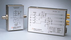
PA-9 Preamplifier
The PA-9 preamplifier is ideal for high-frequency performance with high-impedance photovoltaics such as cryogenically cooled InSb and Ge. The PA-9 offers low current noise and ultra-low voltage noise. However, its relatively high DC offset voltage makes it less suitable for DC applications than other Judson preamps. The PA-9 has fixed gain. When ordered with a detector, the preamp is matched to the detector for maximum gain and sensitivity. Alternatively, the customer may specify gain or minimum required bandwidth. Bandwidth is a function of detector resistance and capacitance as well as preamp gain (Figs. 3 and 4).
 Click for more PA-9 information.
Model | 1st Stage Gain (V/A) | 1st Stage Bandwidth (Maximum) |
PA-9-70 | 107 | DC to 100KHz |
PA-9-60 | 106 | DC to 300KHz |
PA-9-50 | 105 | DC to 750KHz |
PA-9-44 | 2.5x10⁴ | DC to 1MHz |
Typical Specifications Model PA-9 Preamplifiers
2nd Stage Gain | 20 | dB |
Voltage Noise Density @1KHz | 6.5 | nV Hz-1/2 |
Voltage Noise from 0.1 to 10 Hz | 1.0 | µVpp |
Current Noise Density @ 1KHz, 1E7 Gain † | 0.04 | pA Hz-1/2 |
Input Offset Voltage | ± 10 | mV |
Input Bias Curren | t | ± 1 pA | |
Maximum Output | 1st stage = 6
2nd stage = 10 | Vp |
p |
ance | < 50 | W |
Power Requirements | ±12 or ±15
20 | VDC
mA |
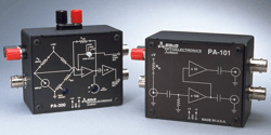
PA-5, PA-6, PA-7 Preamplifiers
Current Mode Preamplifiers convert the current output of a photovoltaic Ge, InAs, or InSb detector into a voltage output. They amplify the signal for subsequent use with oscilloscopes, lock-in amplifiers, or A-to-D converters. Three different preamp models each offer specific advantages, depending on detector type and bandwidth requirements. A comparison of preamp noise figure as a function of detector reactance is graphed in Fig. 6. All units (except multi-channel models) have switch-selectable gain.
The PA-7 is an excellent general purpose preamplifier for most high shunt resistance (RD > 25Kohm) detectors, including small area Ge and TE-Cooled InGaAs, Ge, InAs, SWIR PV MCT, and LN2 Cooled InSb. It has extremely low current noise and current offset. For most applications, the PA-7-70 with high gain of 107 V/A offers best performance and versatility. However, for applications where 107 V/A gain is unusable (due to bandwidth or DC saturation), the PA-7-60 or PA-7-50 are suitable alternatives.
The PA-6 is a general purpose preamplifier recommended for intermediate shunt resistance (400ohm<RD<50Kohm) detectors, including large area Ge and TE-Cooled InGaAs, Ge, InAs, MWIR PV MCT, and LN2 Cooled InSb. J16 Series room temperature Ge. The PA-6 has very low voltage noise and offset voltage, which significantly reduces low-frequency noise and DC drift. Standard gain settings are listed in the specification table below; custom gain settings are available.
The PA-5 is recommended for low impedance detectors (RD<400ohm), including InAs and MWIR PV MCT. It has extremely low voltage noise and low voltage offset. However, its high current noise and current offset make it unsuitable for detectors with high impedance. Standard gain is 105, 104, and 103 V/A (switch-selectable). Custom gain settings are available.
5
Click for more information on the PA-5, PA-6 and PA-7.
Model | PA-7 Series | PA-6 Series | PA-5 | Units |
PA-7-70 | | 0 | PA-7-50 | PA-6-60 | PA-6-50 | PA-5-50 |
Transimpedance : (Switch Selected) | High Med Low | 1E7 1E6 1E5 | 1E6 1E5 2.5E4 | 1E5 4 1E4 | 1E6 E5 2.5E4 | 1E5 2.5E4 1E4 | 1E5 4 1E3 | V/A |
Bandwidth | nF | @ High Gain @ Med Gain @ Low Gain | 8 60 150 | 60 1 | 50 200 | 150 200 200 | 60 150 200 | 150 200 200 | 200 200 200 | KHz |
Input Offset Voltage (Vos) Input Bias Current (ib) Voltage Noise Density (en) @1KHz Voltage Noise from 0.1 to 10Hz Current Noise Density (in)@1KHz† | ±250 ±0.001 12 1.5 .04 | ±250 ±0.001 12 1.5 .13 | ±250 ±0.001 12 1.5 .04 | ±100 ±12 4.5 .080 .5 | ±100 12 4.5 .080 .64 | ±80 ±30 1.1 .035 | 1 | V nA nV Hz-1 |
/2 µVp |
p Hz-1/2 |
e Maximum Output Voltage Power Requir | ements | < 100 ± 10 +12V and -12VDC @ 10mA | W Vpp |
Recommended for Detector Series: | J16, J16TE1, J16TE2, J16D, J10D | J16, J12TE2, J12TE3 | J12, J12TE2 | |
Model | # of Channels | Gain (V/A) | Bandwidth (Max) |
C-70 | 4 | 1E7 | DC to 10KHz |
PA-7:4C-60 | 4 | 1E7 | DC to 60KHz |
(Vos) | ±200 | µV |
Input Bias Current (ib) | ±40 | pA |
Voltage Noise Density (en) @1KHz | 18nVHz-1/2 |
Voltage Noise from 0.1 to 10 | Hz | 2 | µVpp |
Current Noise Density† in @ 1KHz | AHz-1/2 |
Output Impedance | < 100 | W |
Maximum Output Voltage | ±10 | Vpp |
Power Requirements PA-7:4C (4 channel) | ±15 @ 40 | VDC ma |
Use with Detector Series: | NIR Arrays |
† At Gain = 1E7 V/A. Lower gains increase Current Noise Density. |
Voltage Mode Preamplifiers
Voltage Mode Preamplifiers may be used with photoconductive HgCdTe or with low-impedance photovoltaics such as InAs. With photoconductive detectors, a constant bias current or constant bias voltage is applied across the detector element. The element changes resistance in response to incident photons, and the resulting change in voltage is amplified by the preamp. A blocking capacitor or DC offset circuit is required to block the constant DC bias. With photovoltaic detectors, the photocurrent generated in the detector induces a voltage across the preamp input impedance. This voltage is amplified. A lower input impedance generally results in faster frequency response, but also adds more noise to the system
.
PA-101 HgCdTe Preamplifier (5 Hz - 1 MHz): The Model PA-101 low-noise voltage preamplifier is recommended for all J15 Series HgCdTe detectors. An external bias resistor is used to set the constant bias current required for PC detector operation. When purchased with a detector, the preamp includes a bias resistor factory-selected for optimum detector performance. When ordering the preamp separately, please specify detector resistance and required bias current.
Click for more PA-101 information.
Preamplifier Equivalent Circuits shown below.
Model | P/N | Gain | Bandwidth (Hz) | Input Noise Voltage (nV Hz-1 | /2) | Input Impedance (ohms) | Max. Output (Load >1Kohm) | p) | Detector Bias | Power Requirement | Case Dimensions (Excluding Connectors) |
(VDC) | (mA) |
PA-101 | 4 | 90113 | 10 | 10Hz to 1MHz | 1.5 | 10K | 1 | 0 | Bui | lt-in | ±15 | 200 | 4.125" x 2.5" x 1.75" |
| | | | | | | | | | | 4.125" x 2.5" x 1.75" |
|
|
|
|
|
|
|
|
|
|
|